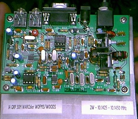
The Iowa QRP Group Presents:
The 30M WARCbler PSK-31
Rig Conversion Kit
By: Fred Spinner, W0FMS and Jeff Woods, W0ODS
(C) Copyright 2001, Fred Spinner and Jeff Woods --
All Rights Reserved
May 14, 2001
|
Part 4--
WARC-Bler Parts List:
| Quantity |
Part |
Marking |
| 6 |
10.141 MHz Crystal |
10.141 / Match Code |
| 1 |
1000 pF Capacitor |
102 |
| 3 |
100 pF Capacitor |
101 |
| 4 |
120 pF Capacitor |
121 |
| 2 |
33 pF Capacitor |
33 |
| 2 |
27 pF Capacitor |
27 |
| 3 |
330 pF Capacitor |
331 |
| 1 |
6.8 uH Inductor |
Silver/Blue/Gold/Grey/Silver |
| 1 |
0.82 uH Inductor |
Silver/Gold/Grey/Red/Silver |
| 1 |
3.3uH Inductor |
Silver/Orange/Gold/Orange/Silver |
| 1 |
8.2 uH Inductor |
Silver/Grey/Gold/Red/Silver |
| 1 |
51 Ohm Resistor |
Green/Brown/Black/Gold |
| 1 |
180 Ohm Resistor |
Brown/Grey/Brown/Gold |
| 1 |
470 KOhm Resistor |
Yellow/Violet/Yellow/Gold |
| 1 |
1.2 KOhm Resistor |
Brown/Red/Red/Gold |
| 2 |
MPS5179 NPN Transistors |
MPS5179 |
| 7" |
Trifilar Magnet Wire |
|
Parts Notes:
Crystals:
Six crystals are provided. These have been matched for better
filter performance. A two digit code is written on the crystal.
The two or three crystals used in the transmit and receive filters, respectively,
should have the same code. The crystal used for Y3, the BFO, need
not be matched.
Inductors:
Four inductors are included with the kit. The WARC-Bler requires
re-use of the original 6.8 uH inductor included originally as L1.
It will be moved to L3. Replacements for the 6.8 uH inductor are
available for $1 (shipped) from Twisted Pair Labs.
The new inductor color codes are somewhat faded, but given the known
values, can be worked out. Contact Twisted Pair Labs for assistance
if the values cannot be determined given the color band information in
the parts list.
Assembly:
The folowing parts from the Warbler kit must be removed or not placed:
Y1-Y6
C6, R7, R8, R11, R12, R13, R15, R16, R17, R18
R6, R8, R15, R16, R17
L1, L2, L3, --IMPORTANT: Do not damage
L1, 6.8 uH. This part will be re-used.
T1
Low Pass Filter:
For L2, wind 13 turns on the same T37-2 core supplied in the original
Warbler kit. For retrofits, remove 10 turns from the Warbler L2.
Place a 330 pF capacitor (331) in the C11 and C12 locations.
The Low-Pass filter has been modified.
(Physically the filter section should look the same as before, but just
with the modified components listed above.)
Transmit Filter:
We're going to replace one component, C6, with three components.
It may look a little ugly, but the filter passband is flat when a proper
match is used.
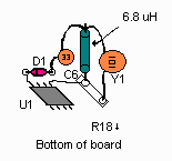 |
Twist one lead of each of the three components together: 33 pF,
6.8 uH and 100pF. Solder the three leads together and trim off excess.
Don't take so much that the strength of the joint is compromised.
More can be removed after it's mounted.
Now, place the free lead of the 6.8 uH inductor in the C6 hole tied
to the SA612. (This is the hole toward the "top" side of the board-- the
top side being the side where the connectors are located.) The other
hole of C6 is filled with the free lead of the 100 pF capacitor.
(The "bottom" side of the board, toward the "NJ-QRP 9/00" writing.)
Ground the 33 pF capacitor by soldering to the grounded lead of D1,
located near C6. |
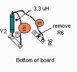 |
A similar operation takes place in the former location of C8.
Twist together and solder a 3.3 uH inductor and a 100 pF capacitor.
Place the other inductor lead in the C8 hole tied to R6. The 100pF
lead goes to the other hole of C8, connecting electrically to Y2.
Place a 27 pF capacitor in the holes formerly used for R6. Remember,
R6 shouldn't be there anymore. If it is, remove it. |
Place a 100 pF capacitor in the C7 location. Place the two crystals
with the same match codes in the Y1 and Y2 positions.
BFO:
Place the unmatched crystal in the Y3 position. The BFO crystal
will have a matching code written on it, but will likely not match any
other crystals in the set.
Transmit Driver Amplifier:
Put an MPS5179 in the places for Q3 and Q4. The pinouts for the
new transistors identical to the 2n4401s they replace. Put a 51 Ohm
resistor in the holes for R8.
The 6.8 uH inductor for L1 is replaced by a 0.82 uH unit. Verify
that C10 is 330 pF. Replace it with an (included) 330pF capacitor
if necessary.)
Re-wind T1 with 6 turns of trifilar wire. This is included
in the Warc-Bler conversion kit. Observe the same polarity used in
the original Warbler. To tin the enameled wire, form a solder ball
on your iron and set the tip of the wire in the ball. Wait
for the wire to heat up. The enamel insulation will begin to bubble
and darken. Slowly move the solder ball up the wire for the desired
tinned length. Clean the tip of your iron, and run your fingernails
over the tinned leads. Tin the leads a second time, and the tinning
should be perfect. Use of a higher temperature iron is helpful,
but not required. 800 degrees F works well, as does a soldering gun.
Scraping away the insulation with sandpaper or a blade is also acceptible--
if you do not nick the wire while scraping!
Receiver Pre-amplifier:
Put a 33 pF capacitor in the C13 position. Put the 6.8 uH inductor
recyled from L1 in the L3 position. Place a 470k resistor in the
R16 position. Place a 180 Ohm resistor in the R15 position.
Place a 1.2k Resistor in the R17 position. Solder a 1000 pF capacitor
in parallel with R17. This is most easily done by using one of the
small capacitors originally intended for C11 or C12 to the R17 leads on
the bottom side of the board. We've included a 1000 pF ceramic disc
capacitor with the kit in the event the (fragile) monolythic caps don't
survive the transplant.
Receiver Filter:
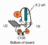 |
The same construction used in the transmit filter will be used again
in the receive filter. Twist together one lead of each of the following:
120 pf, 27 pF, 8.2 uH. The free leg of the 120 pF capacitor goes
in the C18 hole tied to Y6. The inductor lead goes into the other
hole, electrically tied to U2 pin 1. The remaining free lead (27
pF capacitor) is grounded by soldering to the grounded pin of C108 on the
top side of the PCB. |
Populate the rest of the filter by placing 120 pF capacitors in the
positions for C15 to C17 and the remaining crystals in the Y4 to Y6 positions.
This completes the hardware modifications for your Warc-Bler.
Tuning up:
It is necessary to have a calibrated 30m receiver or frequency counter
to accurately set the Warc-Bler's BFO, which affects both receive and transmit.
It is very important to set this for at least 10.1465 MHz or higher
in frequency so that the LO suppression is sufficient for FCC standards!
Power-up the Warc-Bler, terminate the output in 50 ohms, and place
it in transmit mode with no audio drive (remove the audio cable).
Place the counter probe on U2 pin 7 and read the frequency. Tune
C3 to set the frequency of the BFO to 10146.5 KHz. If using a receiver,
a short antenna can be tacked to U2 pin 7 to aid signal pickup. This
is a buffered output and has no effect on the frequency of Y3. Alternatively,
attach the receive audio cable to the computer, and run Digipan.
In DigiPan, set the 30m band configuration to use 10146.5 KHz LSB, and
select the 30m band. Using a HF rig (attached to a dummy load nearby)
to transmit a carrier on 10142.0 KHz using CW or AM, adjust the rig so
the received carrier line lines up at exactly 10142.0 KHz.
Now, connect both audio cables, the RS-232 keying cable, and an antenna
or dummy load. Place the rig in transmit and advance the PC's line
out audio to the point where output power or supply current begins to decrease.
Back off the input signal level so the drive is below the max level.
A simple DC milliammeter in series with the Warc-Bler power supply is sufficient
as a tuning indicator. Nominal input current at 13.8v is 300mA.
The Warc-Bler will produce about 2W at 13.5v and closer to 3W with
a 15V supply. It is good operating practice to rely on the signal
reports of others when adjusting your transmit levels. Don't splatter;
be considerate of other ops. Oh, and have fun WARCbling!!!
THE END RESULT... Pure WARCbling Joy...
NEXT: Conclusion, Appendicies and
Credits.
May 14, 2001
Jeff Woods/Fred Spinner
(HTML Conversion and drawings by Fred Spinner)